Consider the process of manufacturing printed circuit boards at home using a specific example. You need to make two boards. One is an adapter from one type of housing to another. The second is the replacement of a large microcircuit with a BGA package with two smaller ones, with TO-252 packages, with three resistors. Board sizes: 10x10 and 15x15 mm. There are several options for making printed circuit boards at home. The most popular - with the help of photoresist and "iron-laser technology".
Instructions for making printed circuit boards at home
You will need
- personal computer with a program for tracing printed circuit boards;
- laser printer;
- thick paper;
- fiberglass;
- iron;
- hacksaw;
- acid for etching the board.
1 Project preparation printed circuit board
Preparing a PCB project. I use the DipTrace program: convenient, fast, high quality. Developed by our compatriots. Very convenient and pleasant user interface, in contrast to the generally recognized PCAD. Free for small projects. Libraries of cases of radio-electronic components, including 3D models. There is a conversion to PCAD PCB format. Many domestic firms have already begun to accept projects in the DipTrace format.
PCB project
The DipTrace program has the ability to see the future creation in volume, which is convenient and visual. This is what I should get (the boards are shown at different scales):

2 markup fiberglass
First, we mark the textolite and cut out the blank for printed circuit boards.

3 Project output on a laser printer
We output the project on a laser printer in a mirror image in the highest possible quality, without skimping on toner. Through long experiments, the best paper for this was chosen - thick matte paper for printers. You can try using photo paper or buy special thermal paper.

4 Transferring a project on fiberglass
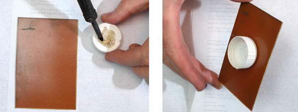
Clean and degrease the board blank. If there is no degreaser, you can walk on the copper foil of fiberglass with an ordinary eraser. Next, using an iron, we “weld” the toner from the paper to the future printed circuit board. I hold for 3-4 minutes under slight pressure, until the paper turns slightly yellow. I set the heat to max. I put another sheet of paper on top for more even heating, otherwise the image may “float”.
An important point here is the uniformity of heating and pressure and the heating time. If the iron is underexposed, then the print will be washed off during etching, and the tracks will be corroded by acid. If overexposed, then nearby conductors can merge with each other.

5 We remove the paper from the workpiece
After that, put the blank with the paper stuck to it in the water. You can not wait until the textolite cools down. Photo paper gets wet quickly, and after a minute or two, you can carefully remove the top layer.

In places where there is a large accumulation of our future conductive tracks, the paper sticks to the board especially strongly. We haven't touched it yet. We give the board a couple more minutes to get wet. Now the rest of the paper is removed with an eraser or rubbing with a finger. You should get a beautiful clean blank with a clearly printed pattern.
 We remove the remnants of paper from the blank of the printed circuit board
 6 Board preparation to pickling
We take out the workpiece. We dry. If somewhere the tracks turned out to be not very clear, you can make them brighter with a thin CD marker or nail polish, for example (depending on what you are going to etch the board with).

It is necessary to ensure that all tracks come out clear, even and bright. It depends on the:
- uniformity and sufficiency of heating the workpiece with an iron;
- accuracy when removing paper;
- quality of textolite surface preparation;
- good luck with paper.
Experiment with different types of paper, different heating times, different types of fiberglass surface cleaning to find the best option in terms of quality. By choosing an acceptable combination of these conditions, in the future you will be able to produce printed circuit boards at home faster and with better quality.
7 Etching printed circuit board
We put the resulting workpiece with future conductor tracks printed on it in acid, for example, in a solution of ferric chloride. We'll talk more about other types of etching. We poison 1.5 or 2 hours. While we are waiting, we will cover the bath with a lid: the fumes are quite caustic and toxic.

8 flushing printed circuit board
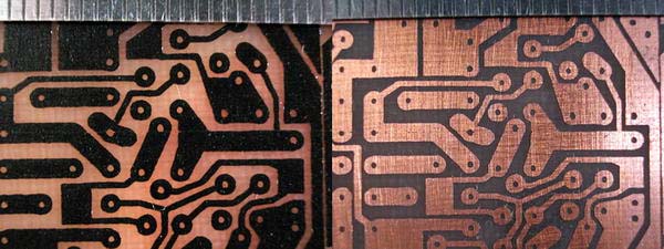
We take out the finished boards from the solution, rinse, dry. Toner from a laser printer is wonderfully washed off the board with acetone. As you can see, even the thinnest conductors with a width of more than 0.2 mm came out quite well. There is very little left.

8 Tinning printed circuit board
We process manufactured printed circuit boards. We wash off the remains of the flux with gasoline or an alcohol-gasoline mixture.
It remains only to cut out the boards and mount the radio elements!
findings
With a certain skill, the “laser-ironing method” is suitable for the manufacture of simple printed circuit boards at home. Conductors from 0.2 mm and thicker are clearly obtained. The time for preparation, experiments with the selection of the type of paper and temperature of the iron, etching and tinning takes about 2 to 5 hours. When you find the optimal combination, the time spent on making the board will be less than 2 hours. This is much faster than ordering boards from a company. Cash costs are also minimal. In general, for simple budget amateur radio projects, the method is recommended for use.
Since I'm an engineering student, I often make projects at home with fairly simple electronic circuits, and for this I often make PCBs myself.
What is a printed circuit board?
A printed circuit board (PCB) is used for mechanical mounting of radio components and their electrical connection using a conductive pattern, pads and other components etched on the copper layer of a laminated plate.
There are pre-designed copper tracks on the PCB. Properly designing connections through these traces reduces the number of wires used and therefore the amount of damage caused by broken connections. The components are mounted on the PCB by soldering.
Creation methods
There are three main ways to make printed circuit boards with your own hands:
- LUT PCB manufacturing technology
- Laying tracks manually
- Etching on a laser machine
The laser etching method is industrial, so I will talk more about the first two manufacturing methods.
Step 1: Create the PCB layout
Typically, wiring is done by converting the circuit diagram using special programs. There are many free programs in the public domain, for example:
I created the layout using the first program.
Do not forget in the image settings (File - Export - Image) select DPIG 1200 for the best image quality.
Step 2: Board materials

(text on photo):
- Magazines or promotional brochures
- Laser printer
- regular iron
- Copper Coated Laminate for PP
- pickling solution
- foam sponge
- Solvent (e.g. acetone)
- Wire in plastic insulation
You will also need: permanent marker, sharp knife, sandpaper, paper towels, cotton wool, old clothes.
I will explain the technology using the example of manufacturing a PP touch switch with IC555.
Step 3: Print out the wiring

Print the wiring diagram on a sheet of A4 glossy or photo paper on a laser printer. Do not forget:
- You need to print the image in mirror image
- Select "Print All Black" in both PCB design software and laser printer settings
- Make sure the image will be printed on the glossy side of the paper.
Step 4: Cut out the board from the laminate


Cut out a piece of laminate sheet the same size as the board layout image.
Step 5: Sanding the Board

Scrub the foil side with a steel wool or the abrasive side of a dishwashing sponge. This is necessary to remove the oxide film and the photosensitive layer.
On a rough surface, the image fits better.
Step 6: Schematic Options


Option 1:
LUT: transfer of an image printed on a glossy layer of paper onto a foil layer of a laminate. Place the printed image on a horizontal surface with the toner facing up. Lay the board on top of the copper layer on the image. The image should be positioned exactly relative to the edges. Fasten the laminate and the image on both sides with tape so that the paper cannot move, the sticky layer of the tape should not get on the copper coating.
Option 2:
Marking the traces with a permanent marker: Using the printed wiring as a sample, mark the circuit on the copper layer of a piece of laminate, first with a pencil, then trace with a permanent black marker.
Step 7: Smoothing Out The Image


- The printed image must be ironed. Heat up the iron to maximum temperature.
- put a clean, unnecessary cloth on a flat wooden surface, put the future board on it with the copper layer up with the circuit image pressed against it.
- on one side, press the board with a hand with a towel, on the other, press it with an iron. Hold the iron for 10 seconds, then start ironing with paper, pressing a little, for 5-15 minutes.
- iron the edges well - with pressure, slowly moving the iron.
- a long press works better than constantly ironing.
- the toner should melt and stick to the copper layer.
Step 8: Cleaning the Board


After ironing, place it in warm water for about 10 minutes. The paper will get wet and can be removed. Remove paper at a low angle and preferably without residue.
Sometimes pieces of tracks are removed with paper.
The white rectangle in the photographs marks the place where the tracks were poorly transferred and then restored with a black permanent marker.
Step 9: Etching


When pickling, you need to be extremely careful.
- put on rubber gloves or plastic-coated gloves first
- cover the floor with newspapers just in case
- fill the plastic box with water
- add 2-3 teaspoons of ferric chloride powder to the water
- soak the board in the solution for about 30 minutes
- ferric chloride will react with copper and copper, not protected by a layer of toner, will go into solution
- to check how the internal parts of the board are being etched, remove the board from the solution with pliers, if the inside has not yet been cleaned of copper, leave it in the solution for some more time.
Stir the solution lightly to make the reaction more active. The solution produces copper chloride and iron chloride.
Check every two to three minutes to see if all of the copper has been etched off the board.
Step 10: Safety


Do not touch the solution with bare hands, be sure to use gloves.
The photo shows how the etching takes place.
Step 11: Solution Disposal
The pickling solution is toxic to fish and other aquatic organisms.
Do not pour the used solution down the sink, it is illegal and can ruin the pipes.
Dilute the solution to reduce the concentration and only then drain into the public sewer.
Step 12: Finishing the Manufacturing Process


The photo shows for comparison two printed circuit boards made using a LUT and a permanent marker.
put a few drops of solvent (you can use nail polish remover) on a cotton swab and remove the remaining toner from the board, you should be left with only copper tracks. Proceed with care, then dry the board with a clean cloth. Cut the board to size and sand the edges with sandpaper.
Drill mounting holes and solder all components to the board.
Step 13: Conclusion
- Laser-ironing technology is a very effective way to make printed circuit boards at home. If you do everything carefully, each track will turn out clear.
- Routing with a permanent marker is limited by our artistic skills. This method is suitable for the simplest circuits, for something more complex it is better to make the board in the first way.
Recently, radio electronics as a hobby in the world is gaining popularity, people are becoming interested in creating electronic devices with their own hands. There are a huge number of circuits on the Internet, from simple to complex, performing various tasks, so everyone can find in the world of radio electronics what they like.
An integral part of any electronic device is the printed circuit board. It is a plate of dielectric material, on which copper conductive tracks are applied that connect electronic components. Each of those who wish to learn how to assemble electrical circuits in a beautiful way must learn how to make these same printed circuit boards.
There are computer programs that allow you to draw a pattern of printed circuit board tracks in a convenient interface, the most popular of them is. The layout of the printed circuit board is carried out in accordance with the circuit diagram of the device, there is nothing complicated in this, it is enough just to connect the necessary parts with tracks. In addition, many circuit diagrams of electronic devices on the Internet already come with ready-made printed circuit board drawings.
A good printed circuit board is the key to a long and happy operation of the device, so you should try to make it as accurately and efficiently as possible. The most common method of making printed ones at home is the so-called "", or "laser-ironing technology". It has gained wide popularity because it does not take much time, does not require scarce ingredients and is not so difficult to learn. Briefly, LUT can be described as follows: let's say there is a pattern of tracks drawn on a computer. Next, this pattern must be printed on special thermal transfer paper, transferred to a textolite, then etched off excess copper from the board, drilled holes in the right places and tinned the tracks. Let's break down the whole process step by step:
Printing a board pattern
1) Printing a pattern on thermal transfer paper. You can buy such paper, for example, on Aliexpress, where it costs mere pennies - 10 rubles per A4 sheet. Instead, you can use any other glossy paper, for example, from magazines. However, the quality of toner transfer from such paper may be much worse. Some use Lomond glossy photo paper, a good option, if not for the price - such photo paper costs much more. I recommend trying to print the drawing on different papers, and then compare with which one you get the best result.
Another important point when printing a picture is the printer settings. It is imperative to turn off toner saving, but the density should be set to the maximum, because the thicker the toner layer, the better for our purposes.

You also need to take into account such a moment that the picture will be transferred to the textolite in a mirror image, so you need to foresee whether or not you need to mirror the picture before printing. This is especially critical on boards with microcircuits, because the other side cannot supply them.

Preparing textolite for transferring a pattern onto it
2) The second stage is the preparation of the textolite for transferring the drawing onto it. Most often, textolite is sold in segments 70x100 or 100x150 mm in size. It is necessary to cut off a piece suitable for the dimensions of the board, with a margin of 3-5 mm along the edges. It is most convenient to cut textolite with a hacksaw for metal or a jigsaw, in extreme cases it can be cut off with scissors for metal. Then, this piece of textolite should be wiped with fine sandpaper or a hard eraser. Minor scratches form on the surface of the copper foil, this is normal. Even if initially the textolite looks perfectly even, this step is necessary, otherwise it will be difficult to tin it later. After sanding, the surface must be wiped with alcohol or a solvent to wash off dust and greasy marks from hands. After that, you can not touch the copper surface.


Transferring the pattern to the prepared textolite
3) The third stage is the most responsible. It is necessary to transfer the pattern printed on thermal transfer paper to the prepared textolite. To do this, cut the paper as shown in the photo, leaving reserves at the edges. We put paper on a flat wooden board with the pattern up, then we apply textolite on top, with copper to the paper. We bend the edges of the paper as if it were hugging a piece of textolite. After that, carefully flip the sandwich so that the paper is on top. We check that the drawing has not shifted anywhere relative to the textolite and put a clean piece of ordinary office white paper on top so that it covers the entire sandwich.


Now it remains only to heat the whole thing thoroughly, and all the toner from the paper will be on the textolite. You need to attach a heated iron on top and heat the sandwich for 30-90 seconds. The heating time is selected experimentally and largely depends on the temperature of the iron. If the toner went badly and remained on the paper, you need to keep it longer, if, on the contrary, the tracks are transferred, but smeared, this is a clear sign of overheating. It is not necessary to put pressure on the iron, its own weight is enough. After warming up, you need to remove the iron and iron the workpiece that has not yet cooled down with a cotton swab, in case the toner did not pass well when ironing with an iron in some places. After that, it remains only to wait until the future board cools down and remove the thermal transfer paper. It may not work the first time, it does not matter, because experience comes with time.
PCB etching
4) The next step is etching. Any area of copper foil that is not covered by the toner must be removed, leaving the copper under the toner untouched. First you need to prepare a solution for etching copper, the simplest, most affordable and cheapest option is a solution of citric acid, salt and hydrogen peroxide. In a plastic or glass container, stir one to two tablespoons of citric acid and a teaspoon of table salt into a glass of water. Proportions do not play a big role, you can pour it on the eye. Mix thoroughly and the solution is ready. You need to put a board in it, tracks down to speed up the process. You can also slightly warm the solution, this will further increase the speed of the process. After about half an hour, all excess copper will be etched away and only tracks will remain.


Rinse toner from tracks
5) The hardest part is over. At the fifth stage, when the board is already etched, you need to wash off the toner from the tracks with a solvent. The most affordable option is female nail polish remover, it costs a penny and almost every woman has it. Common solvents such as acetone can also be used. I use petroleum solvent, although it stinks a lot, it does not leave any black stains on the board. In extreme cases, you can remove the toner by rubbing the board well with sandpaper.

Drilling holes on the board
6) Drilling holes. You will need a small drill with a diameter of 0.8 - 1 mm. Ordinary high speed steel drills quickly become dull on PCB, so it is best to use tungsten carbide drills, although they are more fragile. I drill the boards with an old hair dryer motor with a small collet chuck, and the holes come out clean and burr-free. Unfortunately, at the most inopportune moment, the last carbide drill broke, so only half of the holes were drilled in the photographs. The rest can be drilled later.


Tin tracks
7) It remains only to tin the copper tracks, i.e. cover with solder. Then they will not oxidize over time, and the board itself will become beautiful and shiny. First you need to apply flux to the tracks, and then quickly crawl over them with a soldering iron with a drop of solder. You should not apply an excessively thick layer of solder, then the holes may close, and the board will look sloppy.

This completes the PCB manufacturing process, now you can solder parts into it. The material was provided for the Radio Scheme website by Mikhail Gretsky, [email protected]
Discuss the article MANUFACTURING OF PRINTED BOARDS WITH LUT
Laser ironing technology (LUT for short) is a simple and common method for drawing and manufacturing printed circuit boards at home. This method is available and beneficial for both beginner radio amateurs and experienced craftsmen. The advantages of this method are the low cost of materials, the availability and ease of doing it yourself.
PCB stencil production
 First you need to separate the tracks in special programs for tracing and drawing boards. There are many programs for this purpose, such as Sprint Layout, Pcad, Eagle and Deep Trace. After dividing the tracks on the board, you should print the circuit, be sure to turn off toner saving.
In some cases, it is necessary to print the pattern in a mirror image so that the pins on the board match the pinout of the details, for example, microcircuits in the smd version. For convenience, it is necessary to create a board outline so that after etching it is easier to process the edges of the board, giving them an aesthetic appearance. Then you should remove unnecessary layers for etching or set two layers for tracks and silkscreen in the settings. For reliability, you can print several samples, for possible unsuccessful attempts. You can use any paper with a glossy finish for printing.
Watch a detailed video on making a printed circuit board with your own hands (LUT Technology)
Transferring a drawing to a board
Then you will need an iron, sandpaper, a wooden cutting board and a bath of soapy water. It is necessary to prepare a piece of textolite or getinax suitable for the board, as well as sandpaper of medium grit. Next, you should carefully remove dust and dirt, attach a piece with the print of the board so that the pattern is in the middle of the workpiece. Then wrap tightly, put on a wooden board, put a hot iron on top. The baking temperature of the toner is about 100-180 degrees. Therefore, the temperature of the iron should first be set experimentally, as well as the duration of exposure to the workpiece.
Read also: Voltage stabilizer for a gas boiler: functions, types, selection criteria
After this process, the board must be lowered into a bath of water, with the addition of some kind of soapy solution or dishwashing detergent. You should wait until the paper rots off, 10 minutes is enough. After that, carefully it is necessary to tear it off. If there are poorly printed places, you can correct it with a water-resistant marker.
Board etching
There are many solutions for etching circuit boards, but in this article a solution of hydrogen peroxide with citric acid was used for etching. You should lower the board into the solution and watch the etching reaction, sometimes the reaction is so fast and violent that you can feel the heat from the board at the end of the process. After etching the board, you can see the result - the places that were not covered with toner were deprived of the copper layer, only the tracks and characters that were under the toner layer remained. Next, you will need Solvent 646 and a cloth, such as a disposable cloth or dusting cloth. It is necessary to slightly moisten a rag in the solvent, and wipe the toner from the surface of the workpiece.

Workpiece tinning
The next step in the process is tinning the tracks. Rose alloy was used for this workpiece, unlike Wood's alloy, it does not have cadmium and therefore is not so toxic. The advantage of this tinning method over others is the accuracy and aesthetic appearance of the product. Since the Rose alloy melts at a temperature of +94 degrees, liquid glycerin is used to increase the boiling point, which can be purchased at any pharmacy for a penny. You also need to add a teaspoon of citric acid - it serves as a kind of flux. You will also need two wooden sticks, those that are served with Chinese food will do. A special tampon made of tissue material is put on the end of one stick. It is also advisable to purchase a small rubber spatula, for example, from an auto store.
Read also: Hydraulic accumulator for water supply: types, tips on how to choose. Do-it-yourself hydraulic accumulator
 So, you need to pour a little water into a metal cup, so that it is enough to cover the entire board, plus 3-4 centimeters of water on top, add about a teaspoon of glycerin, sometimes it may take more - you need to install empirically. Then add citric acid, then send the board. Then you have to wait until the solution boils, then, holding the workpiece with a stick with a hard edge, add one granule of Rose alloy there.
After the alloy has become liquid, in the form of a light drop similar to mercury, you should drive this drop with a swab with a soft tip over the surface of the board, without sudden movements. It is important to ensure that the alloy covers all areas of the workpiece prepared for tinning. You can take it out and check it visually, for looseness of individual sections. If necessary, repeat the procedure by throwing another alloy granule. Upon completion of the tinning of the board, you should take out a rubber spatula and, holding the board with a stick, remove excess metal on the surface of the workpiece directly in boiling water, running the spatula over it. The rest of the Rose alloy can be collected in the same boiling water in one large drop and used next time. The workpiece should be washed with running water and dried.
Homemade printed circuit board
How to make a printed circuit board at home using laser ironing technology. This refers to the thermal transfer of toner from paper to the metallization surface of the future printed circuit board.
I tried many times to make a printed circuit board using laser ironing technology, but I never managed to get a reliable, easily repeatable result. In addition, when manufacturing a board, I need etched holes in the contact pads no larger than 0.5 mm. Subsequently, I use them when drilling, in order to center a drill with a diameter of 0.75 mm.
Marriage manifests itself in the form of a shift or change in the width of the tracks, as well as in the unequal thickness of the toner remaining on the copper foil after removing the paper. In addition, when removing the paper before etching, it is problematic to clean each hole in the toner from cellulose residue. As a result, when etching a printed circuit board, there are additional difficulties that could only be avoided by doing the opposite. http://oldoctober.com/en/
I suppose that the reason for the marriage is as follows.
Paper, heated to a high temperature, begins to warp. While the temperature of foil fiberglass is always slightly lower. The toner is partially fixed to the foil, but remains melted on the paper side. When warped, the paper shifts and changes the original shape of the conductors.
At the very beginning, I want to warn that the technology is not without certain drawbacks.
The first one is the absence of a special paper for thermal transfer, instead of which I suggest choosing a suitable paper for self-adhesive labels. Unfortunately, not all paper is suitable. You need to choose one with denser labels, and the substrate has a good, even surface.
The second disadvantage is that the size of the printed circuit board is limited by the dimensions of the soleplate. In addition, not every iron can heat foil fiberglass evenly enough, so it’s better to choose the most massive one.
However, with all these shortcomings, the technology described below allowed me to obtain a stable, easily repeatable result in small-scale production.
The essence of the change in the traditional process is that it is proposed to heat not the paper with toner, but the foil fiberglass itself.
The main advantage is that with this method it is easy to control the temperature in the melting zone of the toner. In addition, the rubber roller allows you to evenly distribute pressure and prevent crushing of the toner. (I write about foil fiberglass everywhere, since I have not tested other materials).
The technology is equally well suited for foil fiberglass of different thicknesses, but it is better to use a material no thicker than one millimeter, since it is easy to cut with scissors.
So, we take a piece of the most shabby foil fiberglass and process it with sandpaper. A very large skin should not be used, as future tracks can be damaged. However, you can not sand if you have a piece of new fiberglass. The copper surface must be thoroughly cleaned and degreased in any case.

We make a stencil for thermal transfer. Why we cut off the necessary piece from a sheet of paper for labels, we separate the labels themselves from the substrate. Leave a piece of label at the beginning of the sheet to prevent the liner from getting stuck in the printer mechanism.
Do not touch the areas on the substrate where the toner will subsequently be applied with your hands.

If the thickness of the foil fiberglass is one or less than a millimeter, then the distance between the edges of the individual boards can be selected as 0.2 mm, if it is larger and you are going to cut the workpiece with a hacksaw, then - 1.5-2.0 mm, depending on the thickness of the web and processing tolerance.

The toner layer I use is the one that is set by default in the printer driver, but “B & W Halftones:” (B / W Halftone) should be selected “Solid” (Solid). In other words, you need to prevent the appearance of a raster. You may not see it on the stencil, but this may affect the thickness of the toner.

We fix the stencil on a piece of foil fiberglass with paper clips. We cling another paper clip to the free edge of the stencil so that it does not come into contact with the iron.
The melting point of different brands of toner is approximately 160-180C. Therefore, the temperature of the iron should be slightly higher by 10-20C. If your iron does not heat up to a temperature of 180C, then you will have to adjust it.

Before heating, the soleplate of the iron must be thoroughly cleaned of grease and other contaminants!
We heat the iron to a temperature of 180-190 degrees and press it tightly against the foil-coated fiberglass as shown in the figure. If the iron is positioned differently, the board may heat up too unevenly, since the iron usually heats up 20-30C more in the wide part. We hold for two minutes.

After that, remove the iron and in one motion, forcefully roll the stencil onto the foil-coated fiberglass using a rubber roller for rolling photos.
If the toner is crushed during packing, that is, the tracks move to the side or change their shape, then the amount of toner in the printer driver should be reduced.
It is necessary that the center of the roller always moves along the center of the board. The handle of the roller must be held in such a way as to prevent the appearance of a force vector directed “around” the handle.

A few more times we strongly roll the stencil and press the resulting “sandwich” with something heavy, having previously laid a newspaper folded several times in order to evenly distribute the weight.
Roll the stencil every time in the same direction. The roller starts moving from the place where the stencil is attached.

After ten minutes, you can remove the press and remove the stencil. Here's what happened.


Now you need to glue something to the back of the board in any way, for which it will later be possible to hold this board during etching. (I use hot glue.)
We poison the board in a solution of ferric chloride.
How to prepare a solution?
If the ferric chloride jar is depressurized, then there is most likely already an over-concentrated solution in there. It can be drained into a pickling dish and a little water added.
If ferric chloride has not yet been covered with water, then you can do it yourself. You can probably get the crystals themselves from the jar, but do not use family silver for this.
Keep in mind that the etching process will not work in a highly concentrated solution, therefore, having received such a solution, you need to add a little water.
As dishes, it is best to use a photo bath made of vinyl plastic, but you can use any other.
The picture shows that the board floats on the surface of the solution due to its surface tension. This method is good because the etching products do not linger on the surface of the board, but immediately sink to the bottom of the bath.

At the very beginning of etching, you need to make sure that there are no air bubbles left under the board. During the etching process, it is desirable to check that the etching proceeds evenly over the entire surface of the board.
If there is any heterogeneity, then you need to activate the process with an old toothbrush or something similar. But this must be done carefully so as not to destroy the toner layer.
Particular attention should be paid to the holes in the pads. The places where the etching process did not start immediately are lighter. In principle, it is enough to achieve a darkening of the entire surface and all holes at the very beginning of the process, and then success is a foregone conclusion.

If the main part of the board was etched in 15 minutes, then you should not increase the total etching time more than twice, that is, more than 30 minutes. Further etching will not only reduce the width of the conductors, but may also partially destroy the toner.
Usually, all 0.5mm holes in the pads are etched in twice the time.
The motor turns a small eccentric, which creates vibrations in the solution (not necessary if you periodically lift and move the board).
Wash off the toner with a swab dipped in acetone.
Here's what happened. On the left, the board is still covered with toner. The track width is 0.4mm.

Now you can remove the burrs that formed on the copper during drilling. To do this, first roll them up with a ball bearing fixed in some convenient mandrel. In this case, the board is best placed on a solid, flat surface. Then, with a fine sandpaper, we remove the oxide from the surface of the copper, if it has formed.

We ludim the workpiece, for which we first cover it with a layer of flux.


I went to the stationery store and took a picture of the packaging with self-adhesive labels. This paper is not suitable for thermal transfer. Although, if there is no other, then this one can be used after some refinement.

The paper that turned out to be the most convenient for thermal transfer was produced by the Finnish company Campas. And since there are no identification marks on small packaging, it is unlikely that it will be possible to identify it without testing.